Qualifier Applications open for January 2027 term, Last date to Apply: January 29, 2027

Qualifier Applications open for January 2027 term, Last date to Apply: January 29, 2027

Degree Level

Digital IC Design

This is a most fundamental Digital Circuit Design course for pursuing a major in VLSI. We discuss transistor level circuit design concepts in great detail. Learning objectives of this course are: • Characterize the key delay quantities of a standard cell • Evaluate power dissipated in a circuit (dynamic and leakage) • Design a circuit to perform a certain functionality with specified speed • Identify the critical path of a combinational circuit • Convert the combinational block to pipelined circuit • Calculate the maximum (worst case) operating frequency of the designed circuit

by Prof. Janakiraman Viraraghavan

Course ID: EE5102

Course Credits: 4

Course Type: Degree

Pre-requisites: None

Course structure & Assessments

For details of standard course structure and assessments, visit Academics page.

Week 1 CMOS inverter fundamentals; CMOS inverter construction, operation, and voltage transfer characteristics.
Week 2 Resistance, capacitance, and transient behavior in CMOS circuits; RC effects and transient response analysis.
Week 3 CMOS power dissipation mechanisms; dynamic power, short-circuit power, leakage power, and stacking effects in low-power design.
Week 4 CMOS combinational circuit design; logic implementation techniques and capacitance considerations in digital circuits.
Week 5 Delay analysis in CMOS circuits; parasitic delay, logical effort, and electrical effort for performance optimization.
Week 6 Gate sizing and buffering techniques; transistor sizing strategies and buffer insertion for delay reduction.
Week 7 Advanced CMOS logic design; asymmetric gates, skewed gates, and ratioed logic circuits.
Week 8 Dynamic logic and timing analysis; dynamic gates, domino logic, and static timing analysis techniques.
Week 9 Sequential circuit design; feedback concepts and implementation of static and dynamic D flip-flops.
Week 10 Timing analysis of sequential systems; setup time, hold time, and timing behavior of latch- and flip-flop-based circuits.
Week 11 High-speed adder architectures; mirror adders, carry skip adders, carry select adders, and square root adders.
Week 12 Multiplier architectures and arithmetic circuits; signed and unsigned multiplication and carry-save multiplier implementation.
+ Show all weeks

Prescribed Books

The following are the suggested books for the course:

Digital Integrated Circuits Jan M. Rabaey, Anantha Chandrakasan and Borivoje Nikolic 2nd Edition, Prentice Hall India, 2003

CMOS VLSI Design, Neil H.E. Weste, David Harris and Ayan Banerjee, 3rd Edition, Pearson Education, 2012

Prof. Vinita Vasudevan's lecture notes on adders and multipliers [http://www.ee.iitm.ac.in/vinita/digic.html]

About the Instructors

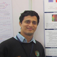
Prof. Janakiraman Viraraghavan
Assistant Professor, Department of Electrical Engineering, IIT Madras

Prof. Janakiraman Viraraghavan is an Assistant Professor at the Department of Electrical Engineering, IIT Madras and is part of the Integrated Circuits and Systems (iCS) group. His research interests include porting machine-learning algorithms on to hardware and statistical analysis in VLSI. He also has a keen interest in Microprocessors and Programming in general.

  less

Other courses by the same instructor: EE1101 - Electronic Systems Thinking and Circuits and EE2103 - Digital System Design